Since the main units, which have less than 14 points, of FBs Series does not provide right expansion module input/output interface, FATAK has developed a special series of analog expansion I/O boards for the units. This series includes analog input expansion board (FBs-B4AD), analog output expansion board (FBs-B2DA), and analog I/O expansion board (FBs-B2A1D). Thus, when customers using the main units have less than 14 points, they will be able to connect to the surrounding analog signals to achieve economic advantages of the application. An introduction of three analog expansion boards is shown in the following:
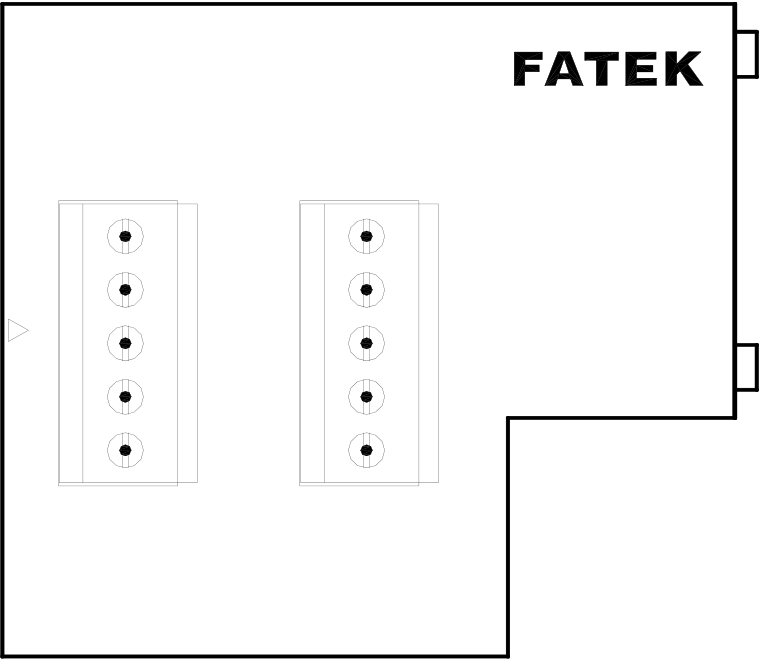
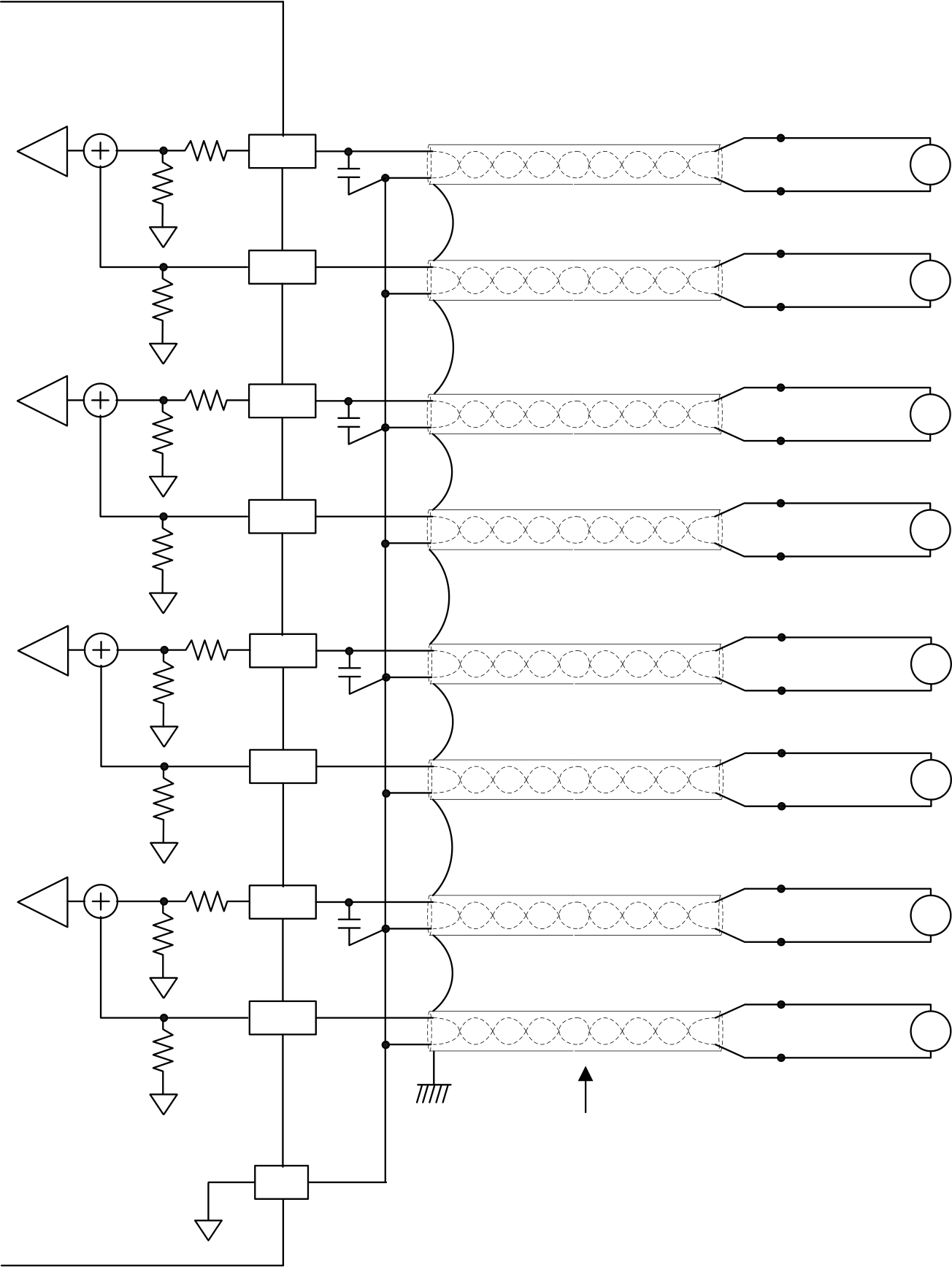
FBs-B4AD is the analog input signal expansion board of FATEK FBs series PLC. It provides 4 channels 12-bit analog input measurement signal (14-bit expression). When applications occurred, it will be able to determine the location of wiring input or output signal type (voltage or current).
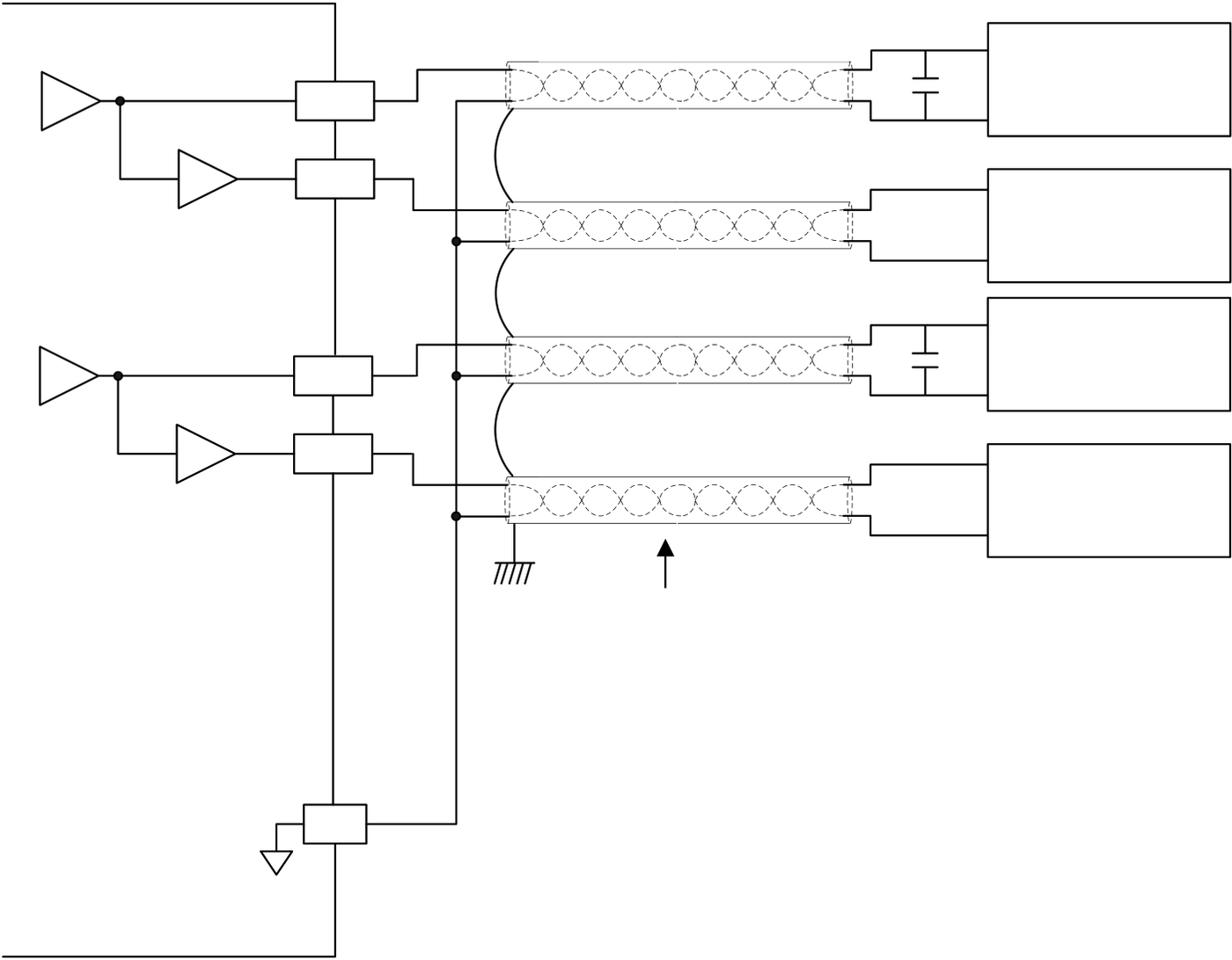
FBs-B2DA is the analog output signal expansion board of FATEK FBs series PLC. It provides 2 channels 12-bit (14-bit expression) analog output signal. When applications occurred, it will be able to determine the location of wiring input or output signal type (voltage or current). For safety, the output signal will be automatically forced to zero (0V or 0mA) when the modules is not serviced by CPU for 0.5 seconds.
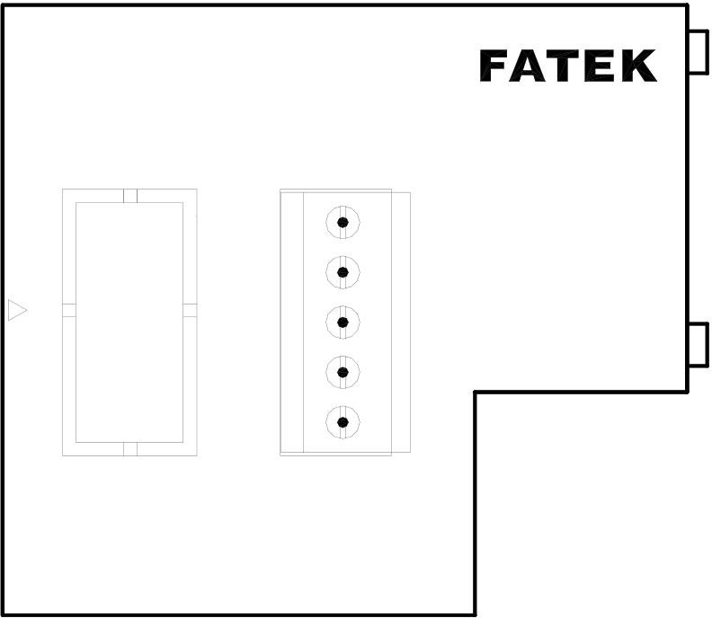
FBs-B2A1D is the analog I/O signal expansion board. It provides 1 channel 12-bit (14-bit expression) analog output signal and measurable 2 channels 12-bit (14-bit expression) analog input signal. When applications occurred, it will be able to determine the location of wiring input or output signal type (voltage or current). For safety, the output signal will be automatically forced to zero (0V or 0mA) when the modules is not serviced by CPU for 0.5 seconds.
19.1Specifications of FBs Analog Expansion Boards
FBs-B4AD Specifications
|
Item |
Specifications |
Remark |
|
|
Input Point |
4 points( 4AD ) |
||
|
Resolution |
12-bit |
||
|
Numeric Expression |
14 bits(0 ~ 16380) |
||
|
Finest Resolution |
2.44mV(Voltage)、4.88µA(Current) |
||
|
I/O Points Occupied |
4 Registers(D4072~D4075) |
||
|
Conversion Time |
Updated each scan |
||
|
Span of Analog Input |
Voltage |
0~10V |
|
|
Current |
0~20mA |
||
|
Accuracy |
Within ±1% of full scale |
||
|
Input Resistance |
100KΩ(Voltage)、125Ω(Current) |
||
|
Internal Consumption |
5V、100mA |
||
|
Working Temperature |
0 ~ 60 ℃ |
||
|
Storage Temperature |
-20 ~ 80 ℃ |
||
FBs-B2DA Specifications
|
Item |
Specifications |
Remark |
|
|
Output Channel |
2 channels ( 2DA ) |
||
|
Resolution |
12-bit |
||
|
Numeric Expression |
14 bits(0 ~ 16380) |
||
|
Finest Resolution |
2.44mV(Voltage)、4.88µA(Current) |
||
|
I/O Points Occupied |
2 Registers(D4076~D4077) |
||
|
Conversion Time |
Updated each scan |
||
|
Span of Analog Output |
Voltage |
0~10V |
|
|
Current |
0~20mA |
||
|
Accuracy |
Within ±1% of full scale |
||
|
Internal Consumption |
5V、120mA |
||
|
Working Temperature |
0 ~ 60 ℃ |
||
|
Storage Temperature |
-20 ~ 80 ℃ |
||
|
FBs-B2A1D Specifications |
|
Detailed Analog Input Specifications |
|||
|
Item |
Specifications |
Remark |
|
|
Input Channel |
2 channels( 2AD ) |
||
|
Resolution |
12-bit |
||
|
Numeric Expression |
14 bits(0 ~ 16380) |
||
|
Finest Resolution |
2.44mV(Voltage)、4.88µA(Current) |
||
|
I/O Points Occupied |
2 Registers (D4072~D4073) |
||
|
Conversion Time |
Updated each scan |
||
|
Span of Analog Input |
Voltage |
0~10V |
|
|
Current |
0~20mA |
||
|
Accuracy |
Within ±1% of full scale |
||
|
Detailed Analog Output Specifications |
|||
|
Item |
Specifications |
Remark |
|
|
Output Channel |
1 channel( 1DA ) |
||
|
Resolution |
12-bit |
||
|
Numeric Expression |
14 bits(0 ~ 16380) |
||
|
Finest Resolution |
2.44mV(Voltage)、4.88µA(Current) |
||
|
I/O Points Occupied |
1 Register (D4076) |
||
|
Conversion Time |
Updated each scan |
||
|
Span of Analog Output |
Voltage |
0~10V |
|
|
Current |
0~20mA |
||
|
Accuracy |
Within ±1% of full scale |
||
|
Detailed Specifications of Common Parts |
|||
|
Item |
Specifications |
Remark |
|
|
Internal Consumption |
5V、150mA |
||
|
Working Temperature |
0 ~ 60 ℃ |
||
|
Storage Temperature |
-20 ~ 80 ℃ |
||
|
19.2The Procedure of Using FBs Analog Expansion Boards |
Start
There is considerable use of differences between
FBs analog expansion board and analog expansion
module. The signal type of FBs analog expansion
board is not set to pin layout, it is set to wiring. This means that there is different pins fixed signal type. If
——-Please refer to section 19.4 for hardware explanation.
you would like to use current or voltage, you would
have to set to the correct pin wiring first. You cannot
adjust pin layout afterword.
Analog Input: Directly read the value of register to
obtain the analog input reading.
Analog Output: Directly fill the output value into the
output register to acquire the corresponding analog
output voltage and current.
End
|
19.3Address Allocation of FBs Analog Expansion Boards |
The address allocation of analog expansion board also has difference to FBs series analog expansion module. The occupied analog expansion board system resources is no longer numerical input register (IR register) R3840~R3903 or numerical output register (OR register) R3904~R3967, but a data register D4072~D4075 (analog input expansion board) or D4076~D4077 (analog output expansion board). The three types of analog expansion boards occupied the resources are listed in below.
Meanwhile, after WinProladder connect with PLC, it will automatically detect and configure the register. Users may refer to the I/O Module Number Configuration provided by WinProladder in order to find out the exact I/O address of each expansion module to facilitate programming.
|
I/O allocation of FBs-B4AD |
|
Channel |
Occupied I/O Resources |
|
|
Analog Input |
CH0 |
D4072 ( 0 ~ 16380 ) |
|
CH1 |
D4073 ( 0 ~ 16380 ) |
|
|
CH2 |
D4074 ( 0 ~ 16380 ) |
|
|
CH3 |
D4075 ( 0 ~ 16380 ) |
|
|
I/O allocation of FBs-B2DA |
|
Channel |
Occupied I/O Resources |
|
|
Analog Output |
CH0 |
D4076 ( 0 ~ 16380 ) |
|
CH1 |
D4077 ( 0 ~ 16380 ) |
|
|
I/O allocation of FBs-B2A1D |
|
Channel |
Occupied I/O Resources |
|
|
Analog Input |
CH0 |
D4072 ( 0 ~ 16380 ) |
|
CH1 |
D4073 ( 0 ~ 16380 ) |
|
|
Analog Output |
CH0 |
D4076 ( 0 ~ 16380 ) |
|
19.4Hardware Description of FBs Analog Expansion Boards |
|
FBs-B4AD outlook and top view |
|
VI0+ |
VI2+ |
PROGRAMMABLE |
|
||||||||||||||||||||
|
CONTROLLER |
|||||||||||||||||||||||
|
II0+ |
II2+ |
FBs-B4AD |
|||||||||||||||||||||
|
VI1+ |
VI3+ |
||||||||||||||||||||||
|
II1+ |
II3+ |
||||||||||||||||||||||
|
Gnd |
Gnd |
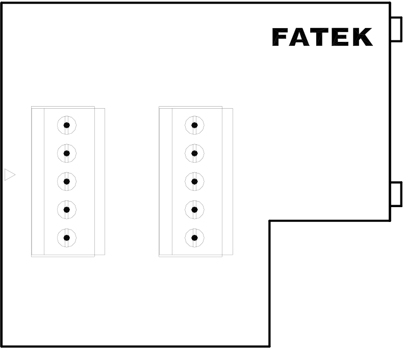
FBs-B2DA outlook and top view
|
PROGRAMMABLE VO0+ IO0+ VO1+ |
|
|||||||||||||
|
IO1+ |
FBs-B2DA |
|||||||||||||
|
Gnd FBs-B2A1D outlook and top view |
||||||||||||||
|
VI0+ |
VO0+ |
PROGRAMMABLE |
|
||||||||||||||||||
|
CONTROLLER |
|||||||||||||||||||||
|
II0+ |
IO0+ |
FBs-B2A1D |
|||||||||||||||||||
|
VI1+ |
|||||||||||||||||||||
|
II1+ |
|||||||||||||||||||||
|
Gnd |
Gnd |






































|
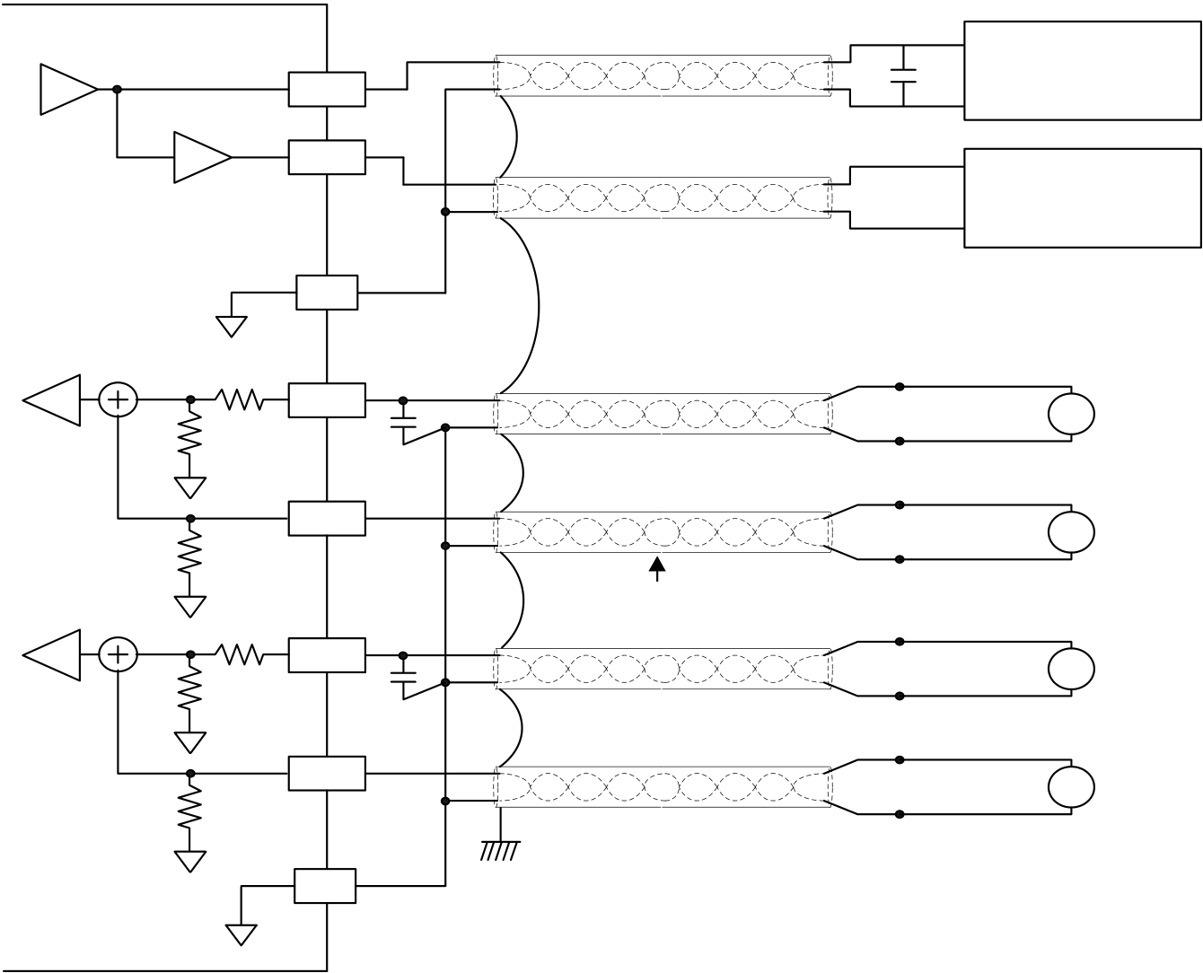
19.5FBs Analog Expansion Boards I/O Circuit Diagram 19.5.1 FBs-B4AD Analog Input Circuit Diagram |

C H 0 Vo l t a g e I n p u t

 O R
C H 0 C u r r e n t I n p u t


C H 1 Vo l t a g e I n p u t

 O R
C H 1 C u r r e n t I n p u t


C H 2 Vo l t a g e I n p u t

 O R

C H 2 C u r r e n t I n p u t



C H 3 Vo l t a g e I n p u t

 O R

C H 3 C u r r e n t I n p u t



Tw i s t e d p a i r w i t h s h i e l d i n g
* 0 . 1 ~ 0 . 4 7 u F c a p a c i t o r ( t o f i l t e r n o i s e ) … … … A d v i c e t o i n s t a l l , b u t n o t n e c e s s a r y ! !


























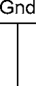



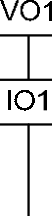


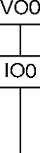

































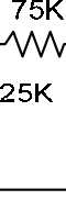
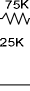
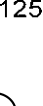




































|
19.5.2 FBs-B2DA Analog Output Circuit Diagram |

C H 0 Vo l t a g e O u t p u t
DEVICE1
C H 0 C u r r e n t O u t p u t
DEVICE2
C H 1 Vo l t a g e O u t p u t
DEVICE3
C H 1 C u r r e n t O u t p u t
DEVICE4
Tw i s t e d p a i r w i t h s h i e l d i n g
|
* 0 . 1 ~ 0 . 4 7 u F c a p a c i t o r ( t o f i l t e r n o i s e ) … … … A d v i c e t o i n s t a l l , b u t n o t n e c e s s a r y ! !
19.5.3 FBs-B2A1D Analog I/O Circuit Diagram |












C H 0 Vo l t a g e O u t p u t
DEVICE1
a n d
DEVICE 2
C H 0 C u r r e n t O u t p u t
C H 0 Vo l t a g e I n p u t

O R
C H 0 C u r r e n t I n p u t
Tw i s t e d p a i r w i t h s h i e l d i n g
C H 1 Vo l t a g e I n p u t
O R
C H 1 C u r r e n t I n p u t
* 0 . 1 ~ 0 . 4 7 u F c a p a c i t o r ( t o f i l t e r n o i s e ) … … … A d v i c e t o i n s t a l l , b u t n o t n e c e s s a r y ! !






















|
19.6FBs Analog Expansion Board I/O Characteristics |
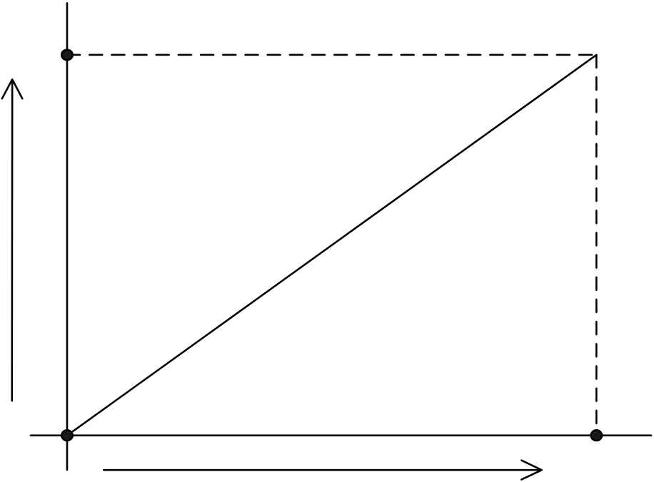
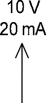
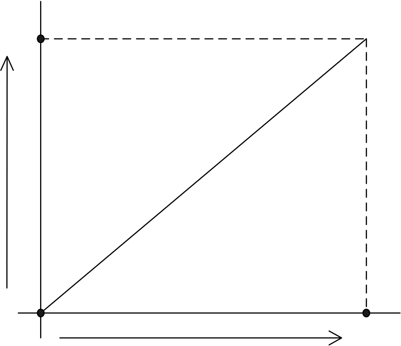
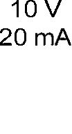
The analog I/O conversion characteristics of these settings are illustrated below. Users can adjust different I/O forms by coordinating the conversion curve with various V/I (Voltage/Current) I/O settings.
|
Figure 1:Analog Input Characteristics Curve |
|
|
|
||
|
|
|
||||





|
Figure 2:Analog Output Characteristics Curve |



Tip: press ← → to switch chapters, Ctrl+K to search