Although FBs Series main unit has been provide analog output module, but allow for the customer who only one point analog output demand. FATEK Automation created the simple and easy analog output module(PWMDA) which to fit various application.
FBs PWMDA Using the theorem of pulse width modulation, cooperate to peripheral output circuit, and then it can transform the different width of digital signal pulse to corresponding analog output voltage(0~10V).
If you want to use PWMDA then you must purchase the PWMDA component form FATEK Automation, and replace to transistor output (the step of replace output component, please refer to chapter 1.1). After finish the component change procedure. Using high speed pulse width modulation instruction (FUN139) to send analog voltage.
|
1.1 PWMDA Component Installation |
FBs-PLC PWMDA component only can be installed in high speed output(Y0、Y2..), because it must match up with FUN139. The shape of PWMDA component and change method shows in below :
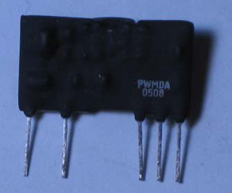
1. If the output component(Y0) were TR(J)-H originally, then remove TR(J)-H directly. And replace to PWMDA component to finish change procedure.
2. If the output component(Y0) were Relay, TR(J), or TR(J)-M originally, then you not only to remove driver transistor (DTC123E), but also to install a SMD resistance(100Ω) in Y0R position.
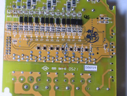
Opening the cover of PLC, take I/O board out and turn it over
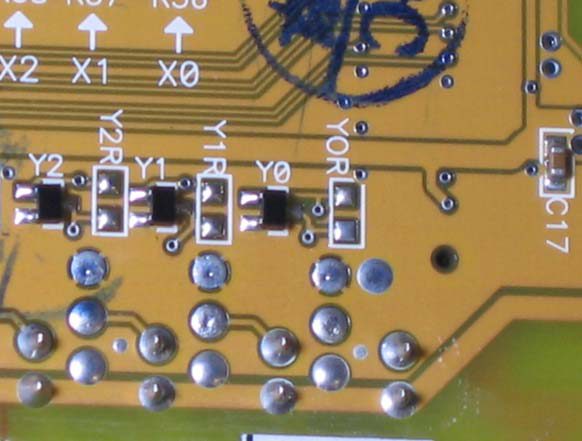
Removed drive transistor Installed the SMD
DTC123E. resistance(100Ω) in Y0R
position.
Before PWMDA component change
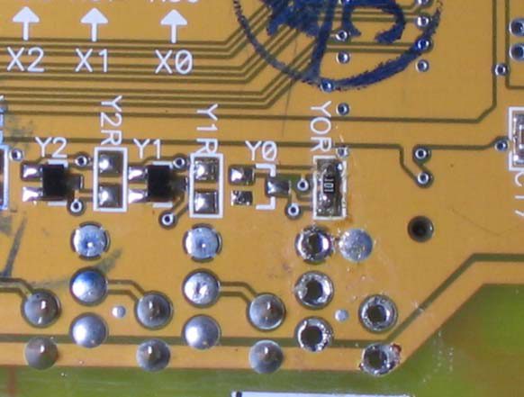
After PWMDA component change
|
• Caution |
|
When Y0 has been finished PWMDA component change, then Y1 won’t be used anymore (because they used the same common ground). After component changed, please pasting the serials number stickers in correct position for recognized easily. |




1.2 Specifications of PWMDA
|
Items |
Specifications |
Remark |
||||||
|
Span of Analog Output |
DC 0~10V |
|||||||
|
Digital output value |
0~1000 |
|||||||
|
Resolution |
10mV(10V/1000) |
|||||||
|
Output resistance |
1K |
|||||||
|
Minimum loading(≥10V output) |
5.2K |
|||||||
|
D/A conversion time |
<50mS |
|||||||
|
Performance curve |
Analog Output
|
|||||||
|
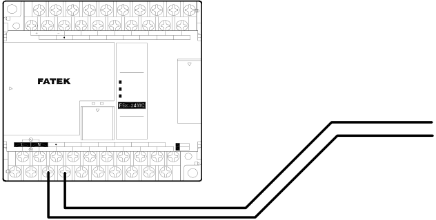
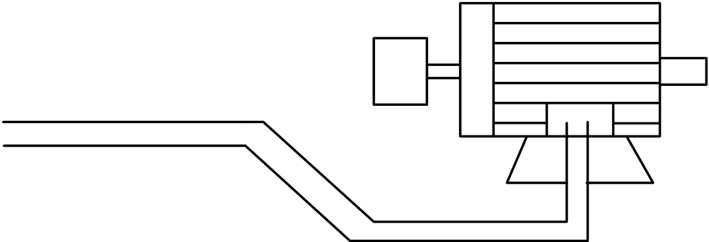
Application Example |
|
|
|
|




|
max. |
24V OUT X0 |
X2 X1 |
X4 X3 |
X5 |
X6 0 |
X7 |
X8 2 3 |
X9 |
X10 |
X11 |
X12 |
X13 |
|
400mA |
S/S |
|||||||||||
|
4 |
5 6 |
6 7 |
||||||||||
|
8 |
9 I |
0 I I |
I2I3
INX ( )
POW
PROGRAMMABLE RUN
|
CONTROLLER |
TX |
RX |
ERR |
|
IN |
AC100~240V |
Y1 |
PORT0 Y2 Y4 |
4 |
0 |
OUT I 2 |
() Y 3 |
Y8 |
SINK |
||
|
4 |
5 6 |
7 Y6 |
|||||||||
|
8 |
9 |
C0 Y0 C2 Y3 C4 C6 Y7 Y9 SRCE




















|
|
|
|
|
|






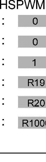
Pw : High speed pulse width modulation (pulse width modulation Æanalog voltage) output point(0=Y0, 1=Y2,…) Op : Output polarity;= 0:Digital output value = 0, Vo=0V;Digital output value = 1000, Vo=10V.
= 1:Digital output value = 0, Vo=10V;Digital output value =1000, Vo=0V.
Rs : Resolution;1=1/1000 (0.1%)。
WR : Working register, it can’t repeat in use.
※ For detail illustration of FUN139, please refer to FBs user’s manual I(Instruction Chapter).
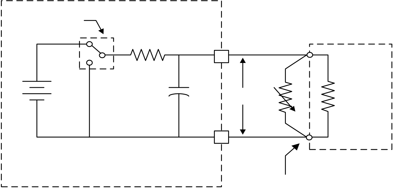
PWMDA hardware diagram & resolution adjustment indication:


|
|
|
|
|
|
|
PWMDA hardware diagram |












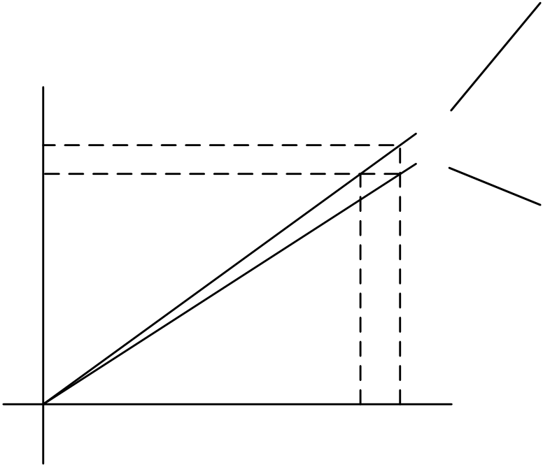
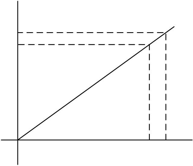
● Adjust through hardware : Firstly setting digital output value as 1000, then to adjust parallel resistance(Rv) to make Vo = 10V.(see curve A in below chart).
● Adjust through software : Firstly setting digital output value as 1000. If Vo≥ 10V then to reduce digital output value until Vo = 10V(see curve B in below chart).
Rin=∞. When digital output value around 879, Vo=10V,
resolution = 11.41mV.
|
|
|
Adjusting the parallel resistance Rv to make Vo=10V when digital |
|
output value = 1000. |



Tip: press ← → to switch chapters, Ctrl+K to search