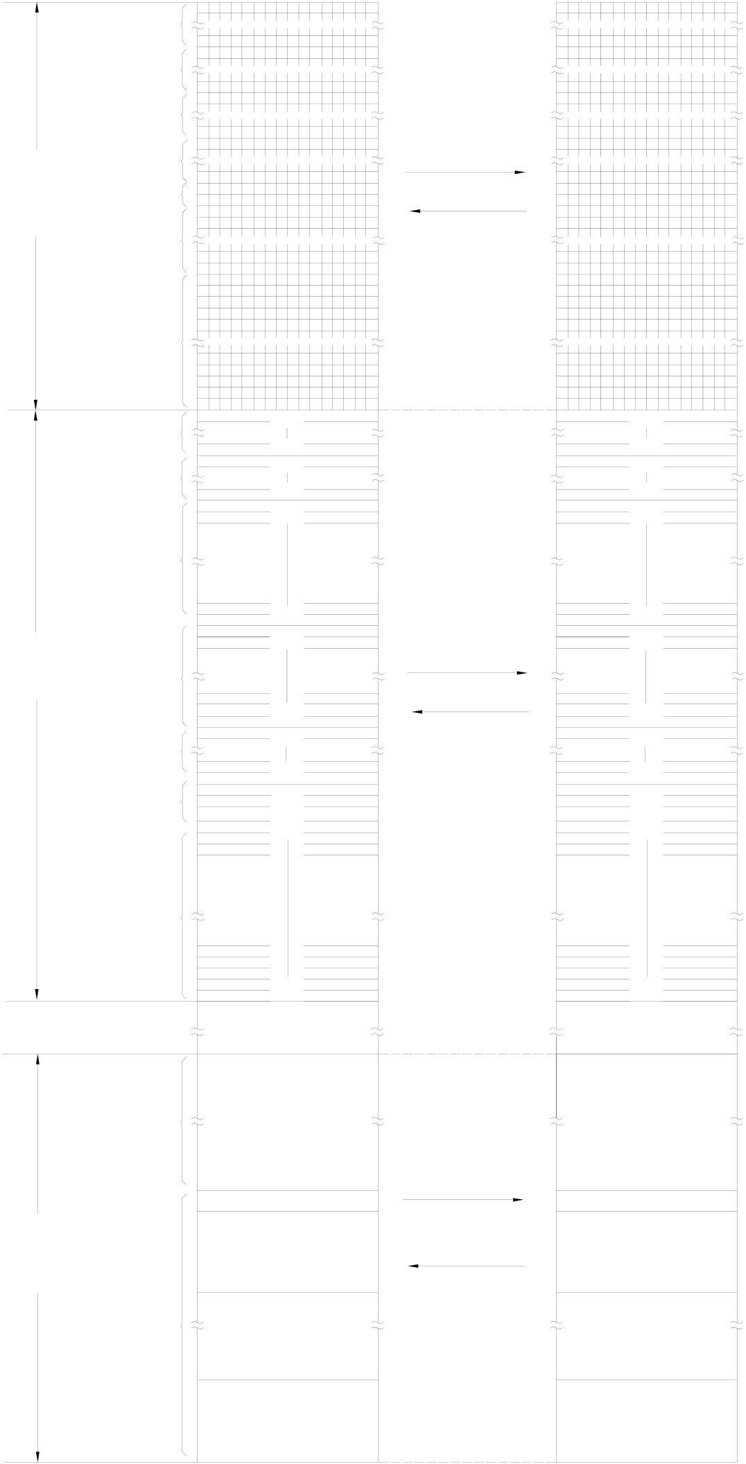
2.1 FBS-PLC MemoryAllocation
Remark:
|
DISCRETE |
X(256) |
X255 |
SRAM |
X0 |
Save status |
FBS-PACK |
X0 |
1. When the Read Only Register (ROR) |
|
X255 |
||||||||
|
has been configured by the user, the |
||||||||
|
Y(256) |
Y0 |
Y0 |
contents of R5000~R8071 (depends |
|||||
|
Y255 |
Y255 |
|||||||
|
T(256) |
T0 |
T0 |
on the quantity of configuration) will |
|||||
|
T255 |
C0 |
T255 |
C0 |
be loaded from the ROR’s during |
||||
|
C(256) |
||||||||
|
STATUS |
TR(40) |
C255 |
S0 |
Load status |
C255 |
S0 |
each time of power up or changing |
|
|
AREA |
||||||||
|
from STOP to RUN mode. |
||||||||
|
(4096) |
S(1000) |
|||||||
|
M(2002) |
S999 |
M0 |
S999 |
M0 |
The user can access the ROR through |
|||
|
the corresponding R5000~R8071. |
||||||||
|
Write operation of function |
instructions are prohibited in this
|
REGISTER |
T(256) |
M2001 |
T0 |
Save Register |
M2001 |
T0 |
ROR area of corresponding R5000~ |
|
C(256) |
T255 |
T255 |
R8071. The others of R5000~R8071 |
||||
|
C0 |
C0 |
||||||
|
C255 |
C255 |
that have not been configured for |
|||||
|
R0 |
R0 |
||||||
|
R(3840) |
ROR, they can work as general |
||||||
|
R3839 |
R3839 |
purpose registers. |
|||||
|
2.There is a dedicated area of program |
|||||||
|
D0 |
D0 |
||||||
|
memory to store the contentsof |
|||||||
|
AREA |
|||||||
|
D(4096) |
D4095 |
Load Register |
D4095 |
Read Only Register. |
|||
|
(20040W) |
|||||||
|
IR , OR |
R3840 |
R3840 |
ROR can be configured up to 3072 |
||||
|
SR(328) |
R4167 |
R4167 |
words in maximum. |
||||
|
R or ROR |
R5000 |
R5000 |
|||||
|
(3072) |
|||||||
|
F0 |
F0 |
F(8192)
F8191 F8191
LADDER LADDER
PROGRAM PROGRAM
(20KW) (20KW)
Save Program
|
LADDER |
LABEL |
Load Program |
LABEL |
|
PROGRAM |
|||
|
(1KW) |
(1KW) |
||
|
AREA |
(32KW)
ROR ROR
(3KW) (3KW)
DOC DOC
(8KW) (8KW)
Memory Buffer in PLC PP/Winproladder
2.2Digital and Register Allocations
〝*〞is default, user configurable
|
Item |
Range |
Remarks |
||||||||
|
X |
Input contact (DI) |
X0~X255 (256) |
Corresponding to external digital input |
|||||||
|
Y |
Output relay (DO) |
Y0~Y255 (256) |
Corresponding to external digital output |
|||||||
|
TR |
Temporary relay |
TR0~TR39 (40) |
||||||||
|
M |
Internal |
Non-retentive |
M0~M799 (800)* |
Can be configured as retentive type |
||||||
|
M1400~M1911 (512) |
||||||||||
|
Retentive |
M800~M1399 (600)* |
Can be configured as non-retentive type |
||||||||
|
Special Relay |
M1912~M2001 (90) |
|||||||||
|
S |
Step |
Non-Retentive |
S0~S499 (500)* |
S20~S499 can be configured as retentive type |
||||||
|
Retentive |
S500~S999 (500)* |
Can be configured as non-retentive type |
||||||||
|
T |
Timer “Time-Up” status contact |
T0~T255 (256) |
||||||||
|
C |
Counter “Counter-Up” status contact |
C0~C255 (256) |
||||||||
|
TMR |
Time current |
0.01STime Base |
T0~T49 (50)* |
T0~T255 numbers for each time base can be adjusted. |
||||||
|
0.1S Time Base |
T50~T199 (150)* |
|||||||||
|
1S Time Base |
T200~T255 (56)* |
|||||||||
|
CTR |
Counter current value register |
Retentive |
C0~C139 (140)* |
Can be configured as non-retentive type |
||||||
|
Non-Retentive |
C140~C199 (60)* |
Can be configured as retentive type |
||||||||
|
Retentive |
C200~C239 (40)* |
Can be configured as non-retentive type |
||||||||
|
Non-Retentive |
C240~C255 (16)* |
Can be configured as retentive type |
||||||||
|
HR |
Data |
Retentive |
R0~R2999 (3000)* |
Can be configured as non-retentive type |
||||||
|
D0~D3999 (4000) |
||||||||||
|
Non-Retentive |
R3000~R3839 (840)* |
Can be configured as retentive type |
||||||||
|
HR |
Retentive |
R5000~R8071 (3072) * |
When not configured as ROR, it can serve normal register (for read/write) |
|||||||
|
Read Only |
R5000~R8071 can be set as ROR ~ default setting is (0)* |
ROR is stored in special ROR area and not occupy program space |
||||||||
|
File Register |
F0~F8191 (8192) |
Save/retrieved via dedicated instruction |
||||||||
|
IR |
Input Register |
R3840~R3903 (64) |
Corresponding to external numeric input |
|||||||
|
OR |
Output Register |
R3904~R3967 (64) |
Corresponding to external numeric output |
|||||||
|
SR |
Special system register |
R3968~R4167 (197) D4000~D4095 (96) |
||||||||
|
0.1 mS High-Speed Timer Register |
R4152~R4154 (3) |
|||||||||
|
HSC |
Hardware (4sets) |
DR4096~DR4110 (4×4) |
||||||||
|
Software(4sets) |
DR4112~DR4126 (4×4) |
|||||||||
|
Calendar Registers |
Minute |
Second |
R4129 |
R4128 |
||||||
|
Day |
Hour |
R4131 |
R4130 |
|||||||
|
Year |
Month |
R4133 |
R4132 |
|||||||
|
Week |
R4134 |
|||||||||
|
FR |
File Registers |
F0~F8191(8192) |
||
|
XR |
Index Registers |
V,Z (2)、P0~P9 (10) |
Remark: During power up or changing operation mode from STOP→RUN, all contents in non-retentive relays or registers will be cleared to 0; the retentive relays or registers will remain the same state as before.
2.3Special Relay Details
|
Relay No. |
Function |
Description |
|
1. Stop, Prohibited Control |
||
|
M1912 M1913 M2001 |
Emergency Stop control Disable external outputs control Disable/Enable status retentive control |
y If 1, PLC will be stopped (but not enter STOP mode) and all outputs OFF. This bit will be cleared when power up or changing operation mode from STOP→RUN. y All external outputs are turn off but the yIf M2001 is 0 or enabled, the Disable/Enable status of all contacts will be reset to enable during power up or changing operation mode from STOP→RUN. yIf M2001 is disabled and force ON, the Disable/Enable status & ON/OFF state of all contacts will remain as before during power up or changing operation mode from STOP→RUN. While testing, it may disable and force ON M2001 to keep the ON/OFF state of disabled contacts, but don’t forget to enable the M2001 after testing. |
|
2. CLEAR Control |
||
|
M1914 M1919 |
Clear Non-Retentive Relays Clear Retentive Relays Function output control |
y Cleared When at 1 If 1, the pulse activated functions within the master control loop will be executed every time while changing 0→1 of master control loop. yIf 0, the functional outputs of some function instructions will memory the output state, even these instructions not been executed. If 1, the functional output of some function instructions without the memory ability. |
|
※ M1918/M1919 can be set to 0 or 1 at will around the whole program to meet the control requirements. |
||
|
Relay No. |
Function |
Description |
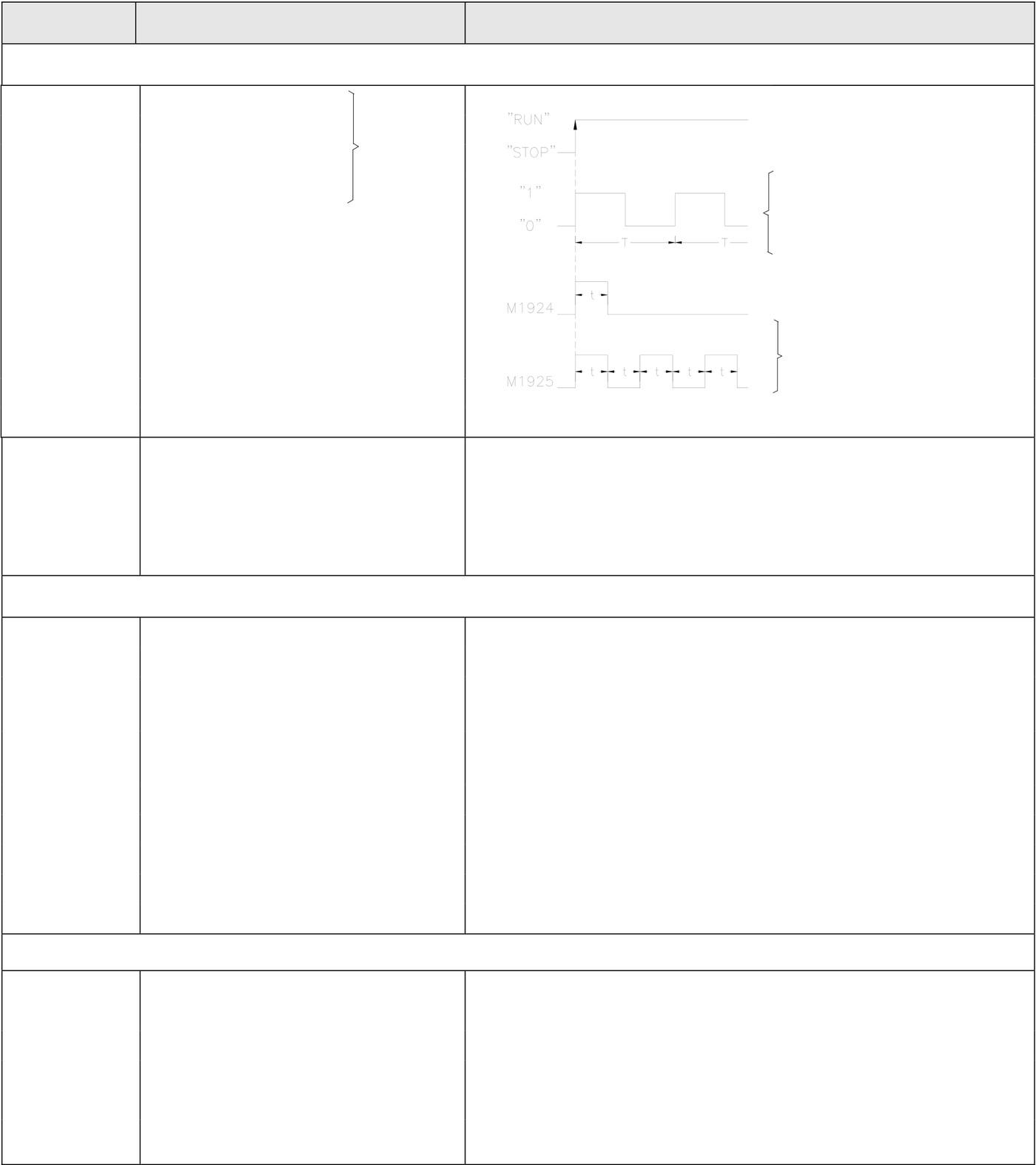
3. Pulse Signals
|
◤M1920 |
0.01S Clock pulse |
c |
c |
T(M1920)=0.01S |
|
◤M1921 |
||||
|
0.1S Clock pulse |
||||
|
◤M1922 |
||||
|
1S Clock pulse |
||||
|
◤M1923 |
||||
|
60S Clock pulse |
T(M1921)=0.1S |
T(M1922)=1S
|
◤M1924 |
Initial pulse (first scan) d |
T(M1923)=60S |
|
|
◤M1925 |
Scan clock pulses e |
d |
|
|
◤M1926 |
=0, PLC is working at STOP mode |
e |
t is the scan time |
|
=1, PLC is working at RUN mode |
|||
|
◤M1927 |
CTS input status of communication |
||
|
y 0:CTS True (ON) |
|||
|
y 1:CTS False (OFF) |
|||
|
port 1 |
|||
|
y When communication port 1 is used to connect with the printer |
|||
or modem, it can use this signal and a timer to detect whether the printer or the modem is ready.
4. Error Messages
|
◤M1928 |
Reserved |
y 1: Indicating no expansion unit or exceed the limit on number of |
|
◤M1929 |
Reserved |
|
|
◤M1930 |
No expansion unit or exceed the limit |
|
|
◤M1931 |
on number of I/O points |
I/O points |
|
Immediate I/O not in the main unit |
y 1: Indicating that Immediate I/O not in the main unit range and |
|
|
◤M1932 |
range |
the main unit cannot RUN |
|
Unused |
||
|
◤M1933 |
System stack error |
y 1: Indicating that system stack error |
◤M1934
│Reserved
◤M1935
5.Port3~Port4 Controls(MC/MN)
|
M1936 |
Port 3 busy indicator |
y 0:Port 3 Busy |
y 1:Port 3 Ready
|
M1937 |
Port 3 finished indicator |
y 1:Port 3 finished all communication transactions |
|
M1938 |
Port 4 busy indicator |
y 0:Port 4 Busy |
y 1:Port 4 Ready
|
M1939 |
Port 4 finished indicator |
y 1:Port 4 finished all communication transactions |
|
Relay No. |
Function |
Description |
|
6. HSC0~HSC1 Controls (MC/MN) |
||
|
M1940 |
HSC0 software Mask |
y 1: Mask y 1: Mask y 1: Port 3 has received and transmitted a message y 1: Port 4 has received and transmitted a message |
|
7. RTC Controls |
||
|
M1952 |
RTC setting RTC installation checking Set value error |
|
|
8. Communication/Timing/Counting Controls |
||
|
M1956 M1957 M1958 M1959 M1960 M1961 M1962 M1963 M1964 |
Selection of Message Frame Interval Detection Time The CV value control after the timer "Time Up" Communication port 2 High Speed Link mode selection Modem dialing signal selection Port 1 busy indicator Port 1 finished indicator Port 2 busy indicator Port 2 finished indicator Modem dialing control |
y 0 :Use system default value as Message Frame Interval Detection Time for Modbus RTU communication protocol y 1:Use the high byte value of R4148 as Message Frame Interval Detection Time for Modbus RTU protocol y 1: Dialing by PULSE when Port 1 connecting wit Modem. y 0:Port 1 Busy |
|
Relay No. |
Function |
Description |
|
M1965 M1966 M1967 M1968 M1969 M1970 M1971 M1972 M1973 M1974 M1975 |
Dialing success flag Dialing fail flag Port 2 High Speed Link working mode selection Step program status Indirect addressing illegal write flag Port 0 status Port 1 status Port 2 status The CV value control after counting “Count-Up” RAMP function slope control CAM function (FUN112) selection |
y 1: Indicating that dialing is successful (when Port 1 is connected with Modem). y 1: Indicating that dialing has failed (when Port 1 is connected with Modem). y 0: Continuous cycle. y 1: One cycle only. It will stop when the last communication transaction is completed (only effective at the master station). y 1: Indicating that there are more than 16 active steps in the step program at the same time. y 1: Indicating that a function with index addressing attempts to write cross over the boundary of different type of data. y 1: Port 0 has received and transmitted a message y 1: Port1 has received and transmitted a message y 1: Port2 has received and transmitted a message y 0: Indicating that the CV value will continue counting up to the upper limit after “Time-Up”. y 1: Indicating that the CV value will stop at the PV value after “Count-Up”(User may control M1973 within the program to control the individual counter) y 0: Time control for ramping y 1: Equivalent slope control for ramping y 1: For the circular applications where the electric CAM switch (FUN112) can support the wrap around situation like the angle from 359° cross to 0° |
|
9. HSC2~HSC7 Controls |
||
|
M1976 |
HSC2 software Mask |
y 1: Mask |
|
M1983 |
HSC4 software Direction HSC5 software MASK HSC5 software Direction HSC6 software Mask |
y 0: Count-up, 1: Count-down |
|
Relay No. |
Function |
Description |
|
10. PSO0~POS3 Controls |
||
|
M1991 M1992 M1993 M1994 M1995 |
Selection of stopping the pulse output (FUN140) PSO0 Busy indicator PSO1 Busy indicator PSO2 Busy indicator PSO3 Busy indicator |
y 0:Immediately stop while stopping pulse output y 1:Slow down stop while stopping pulse output y 0:PSO0 Busy y 0:PSO2 Busy |
|
M1996 |
PSO0 Finished indicator |
y 1:PSO0 finished the last step of motion y 1:PSO1 finished the last step of motion y 1:PSO2 finished the last step of motion y 1:PSO3 finished the last step of motion y 1: Synchronized Multi-Axis |
2.4 Special Registers Details
|
Register No. |
Function |
Description |
|
R3840 |
Input Registers ││ |
For Analog or Numeric inputs |
|
R3904 |
Output Registers ││ |
For Analog or Numeric outputs |
|
R3968 |
Define stimulate Modbus equipment |
|
|
R3981 |
Reserved |
|
|
R4000 |
Reserved |
|
|
R4001 |
Reserved |
|
|
R4002 |
Reserved |
|
|
R4003 |
Define FUN86 temperature reading value at starting/end address |
|
Register No. |
Function |
Description |
|
R4005 |
High Byte:Period of PWM |
For PID temperature control |
|
R4006 |
Threshold value of output ratio for |
For PID temperature control |
|
R4007 |
Threshold value of continuous time for |
For PID temperature control |
|
R4008 |
Maximum temperature for heating loop abnormal detecting |
For PID temperature control |
|
R4009 |
Temperature display in Celsius/Fahrenheit |
=0, Celsius ;=1,Fahrenhelt |
|
R4010 |
Installed temperature sensor flag |
Each bit represents 1 sensor, if bit value = 1 means installed. |
|
R4012 |
PID Temperature control flag |
Each bit represents 1 temperature point, if bit value = 1 means enable control. |
|
R4014 |
Reserved |
|
|
R4015 |
Averaging of temperature value =0, no average on temperature =1, average by two readings =2, average by four readings =3, average by eight readings |
|
|
R4016 |
Reserved |
|
|
R4017 |
Reserved |
|
|
R4018 |
Reserved |
|
|
R4019 |
Number of PASSWORD Retry |
|
|
R4020 |
Control FUN148 instruction forbid to clockwise/anti-clockwise. |
|
|
R4021 |
Reserved |
|
|
R4025 |
Total Expansion Input Registers |
|
Register No. |
Function |
Description |
|
R4026 |
Total Expansion Output Registers Total Expansion Digital Inputs |
|
|
R4029 |
Reserved for system |
|
|
R4030 |
Tables to save or read back the data registers into or from ROM Pack |
When the ROM Pack being used to save the ladder program and data registers, these tables describes which registers will be written into the ROM Pack. The addressed registers will be initialized from ROM Pack while power up. |
|
R4040 |
Reply delay time settings for Port 0 and Port 1 |
Low Byte:For Port 0 (Unit in mS) High Byte:For Port 1 (Unit in mS) |
|
R4041 |
Reply delay time settings for Port 2 and Port 3 |
Low Byte:For Port 2 (Unit in mS) High Byte:For Port 3 (Unit in mS) |
|
R4042 |
Reply delay time settings for Port 4 |
Low Byte:For Port 4 (Unit in mS) High Byte:Reserved for system |
|
R4043 |
Port 3 Communication Parameters Register |
Set Baud Rate, Data bit…of Port 3 |
|
R4044 |
Port 4 Communication Parameters Register |
Set Baud Rate, Data bit…of Port 4 |
|
R4045 |
Transmission Delay & Receive Time-out interval time Setting, while Port 3 being used as the master of FUN151 or FUN150 |
Low Byte:Port 3 Receive Time-out interval time (Unit in 10mS) High Byte:Port 3 Transmission Delay (Unit in 10mS) |
|
R4046 |
Power up initialization mode selection of data registers that has been written into ROM |
=5530H: Don’t initialize the addressed data registers been written into ROM Pack while power up =Others : initialize the addressed data registers been written into ROM Pack while power up |
|
R4047 |
Communication protocol setting for Port1~Port4 |
Set the FATEK or Modbus RTU/ASCII communication protocol |
|
R4048 |
Transmission Delay & Receive Time-out interval time Setting, while Port 4 being used as the master of FUN151 or FUN150 |
Low Byte:Port 4 Receive Time-out interval time (Unit in 10mS) High Byte:Port 4 Transmission Delay (Unit in 10mS) |
|
R4049 |
CPU Status Indication |
=A55AH, Force CPU RUN |
|
R4050 |
Port 0 Communication Parameters Register |
Set Baud Rate of Port 0 |
|
R4051 |
Reserved |
|
|
R4052 |
Indicator while writing ROM Pack |
|
Register No. |
Function |
Description |
|||||
|
R4053 |
Reserved |
||||||
|
R4054 |
Define the master station number of the High-Speed CPU Link network (FUN151 Mode 3) |
If the master station number is 1,it can ignore this register. To set the master station number other than 1 should: Low Byte : Station number |
|||||
|
R4055 |
PLC station number |
y If high byte is not equal 55H, R4055 will show the station number of this PLC y If want to set PLC station number then R4055 should set to: Low Byte : Station number High Byte: 55H |
|||||
|
R4056 |
High Byte :Reserved |
Low Byte: =5AH, can dynamically change the output frequency of High Speed Pulse Output |
|||||
|
R4057 |
Power off counter |
The value will be increased by 1 while power up |
|||||
|
R4058 |
Error station number while Port 2 in High Speed CPU Link |
Used by FUN151 Mode 3 of Port 2 |
|||||
|
R4059 |
Error code while Port 2 in High Speed CPU LINK mode |
Used by FUN151 Mode 3 of Port 2 High byte Low Byte
Error code: 0AH, No response 01H, Framing Error 02H, Over-Run Error 04H, Parity Error |
|
Register No. |
Function |
Description |
|
R4060 R4061 |
Error code of PSO 0 Error code of PSO 1 |
The error codes are: Same as above Same as above |
|
R4064 |
Being completed step number of positioning program |
PSO 0 |
|
R4068 |
FUN147 GP0 vector speed |
|
|
R4070 |
FUN147GP1 vector speed |
|
Register No. |
Function |
Description |
|
R4072 |
Pulse count remaining for output |
Low Word of PSO 0 |
|
R4080 |
Current output frequency |
Low Word of PSO 0 |
|
R4088 |
Current pulse position |
Low Word of PSO 0 |
|
Register No. |
Function |
Description |
|
R4096 |
HSC0 current value Low Word HSC0 current value High Word HSC0 preset value Low Word HSC0 preset value High Word HSC1 current value Low Word HSC1 current value High Word HSC1 preset value Low Word HSC1 preset value High Word HSC2 current value Low Word HSC2 current value High Word HSC2 preset value Low Word HSC2 preset value High Word HSC3 current value Low Word HSC3 current value High Word HSC3 preset value Low Word HSC3 preset value High Word HSC4 current value Low Word HSC4 current value High Word HSC4 preset value Low Word HSC4 preset value High Word HSC5 current value Low Word HSC5 current value High Word HSC5 preset value Low Word HSC5 preset value High Word HSC6 current value Low Word HSC6 current value High Word HSC6 preset value Low Word HSC6 preset value High Word HSC7 current value Low Word HSC7 current value High Word HSC7 preset value Low Word HSC7 preset value High Word |
|
|
R4128 |
Second of calendar |
|
|
R4129 |
Minute of calendar |
|
|
R4130 |
Hour of calendar |
|
|
R4131 |
Day of calendar |
|
|
R4132 |
Month of calendar |
|
|
R4133 |
Year of calendar |
|
|
R4134 |
Day of week of calendar |
|
|
R4135 |
month 十 minute |
|
|
◤ R4136 ◤ R4137 ◤ R4138 |
Current scan time |
y Error < ±1ms |
|
Register No. |
Function |
Description |
||
|
R4139 |
CPU Status |
Bit0 =0, PLC STOP |
||
|
R4140 |
|

|
Register No. |
Function |
Description |
|
R4146 |
Port 1 Communication Parameters Register |
Set Baud Rate, Data bit… of Port 1 |
|
R4147 |
Transmission Delay & Receive Time-out interval time Setting, while Port 1 being used as the master of FUN151 or FUN150 |
Low Byte:Port 1 Receive Time-out interval time (Unit in 10mS) High Byte:Port 1 Transmission Delay (Unit in 10mS) |
|
Register No. |
Function |
Description |
|
R4148 |
Message Frame Detection Time Interval |
.While the communication port being used as the master or slave of Modbus RTU protocol, the system will give the default time interval to identify each packet of receiving message; except this, the user can set this time interval through the high byte setting of R4148 and let M1956 be 1, to avoid the overlap of different packet of message frame. M1956=1, High Byte of R4148 is used to set the new message detection time interval for Port 1~Port 4 (Unit in mS) .While the communication port being used to communicate with the intelligent peripherals through FUN151 (Unit in mS) |
|
R4149 |
Modem Interface Setting & Port0 |
y High Byte of R4149: =AAH, Remote diagnosis by way of Port 1 through Modem connection, it =Others, without above function y Low Byte of R4149: =Others, Port 0 checks station number, it allows multi-drop network for data acquisition. |
|
R4150 |
Power on I/O service delay time setting |
y PLC is ready for I/O service after this delay time while power up. The unit is in 0.01S. The default value is 100. |
|
R4151 |
Circular 1mS time base timer |
y The content of R4151 will be increased by 1 every 1mS. It can be used for a more precise timing application. |
|
R4152 |
Low word of HSTA CV register |
HSTA is high speed timer in 0.1 mS resolution |
|
R4153 |
High word of HSTA CV register |
The HSTA can act as 32-bit cyclic timer or fixed time interrupt timer |
|
R4154 |
PV register of HSTA |
|
Register No. |
Function |
Description |
|
R4155 |
Port 1 & Port 2 without station number checking for FATEK’s external |
y Low Byte of R4155: ≠1,Port 1 checks station number, it allows multi-drop network for data acquisition y High Byte of R4155: |
|
R4156 |
Port 3 & Port 4 without station number checking for FATEK’s external |
y Low Byte of R4156: ≠1,Port 3 checks station number, it allows multi-drop network for data acquisition y High Byte of R4156: ≠1,Port 4 checks station number, it allows multi-drop network for data acquisition |
|
R4157 |
PLC OS Version |
|
|
R4158 |
Port 2 Communication Parameters Register |
Set Baud Rate, Data bit…of Port 2 |
|
R4159 |
Transmission Delay & Receive Time-out interval time Setting, while Port 2 being used as the master of FUN151 or FUN150 |
Low Byte:Port 2 Receive Time-out interval time (Unit in 10mS) High Byte:Port 2 Transmission Delay (Unit in 10mS) |
|
R4160 |
Port2 RX/TX time out setting for High Speed CPU Link |
High Byte of R4160 : |
|
R4161 |
Port 2 Communication Parameters Register |
ySet Baud Rate, Parity…of Port 2 y Data bit is fixed to 8-bit |
|
R4162 |
Fixed time interrupt enable/disable |
B7 |
B6 |
B5 |
B4 |
B3 |
B2 |
B1 |
B0 |
|
control |
100mS50mS10mS5mS 4mS 3mS 2mS1mS |
||||||||
Bit=0, interrupt enabled
Bit=1, interrupt disabled
|
Register No. |
Function |
Description |
|
|
R4163 |
Modem dialing control setting |
y Low Byte of R4163 : |
=1, Ignore the dialing tone and the busy tone when
dialing.
=2, Wait the dialing tone but ignore the busy tone when
dialing.
=3, Ignore the dialing tone but detect the busy tone
when dialing.
=4, Wait the dialing tone and detect the busy tone when
dialing.
=Any other value treated as value equal 4.
y High Byte of R4163 :
The Ring count setting for Modem auto answer
|
R4164 |
V index register |
|
|
R4165 |
Z index register |
|
|
R4166 |
System used |
|
|
R4167 |
Model of main unit |
y Low Byte of R4167: |
=0, 6I + 4O (FBs-10xx)
=1, 8I + 6O (FBs-14xx)
=2, 12I + 😯 (FBs-20xx)
=3, 14I + 10O (FBs-24xx)
=4, 20I + 12O (FBs-32xx)
=5, 24I + 16O (FBs-40xx)
=6, 36I + 24O (FBs-60xx)
=7, 28I + 16O (FBs-44MN)
y High Byte of R4167:
=0, MA
=1, MC
=2, MN
|
Register No. Function |
Description |
|
|
D4000 |
Port 1 User-defined Baud Rate Divisor |
Port 1 user-defined Baud Rate (1125~1152000 bps) D4000 = (18432000/Baud Rate) – 1 |
|
(R4146 must be 56XFH) |
||
|
D4001 |
Port 2 User-defined Baud Rate Divisor |
Port 2 user-defined Baud Rate (1125~1152000 bps) D4001 = (18432000/Baud Rate) – 1 |
|
(R4158 must be 56XFH) |
||
|
D4002 |
Port 3 User-defined Baud Rate Divisor |
Port 3 user-defined Baud Rate (1125~1152000 bps) D4002 = (18432000/Baud Rate) – 1 |
|
(R4043 must be 56XFH) |
||
|
D4003 |
Port 4 User-defined Baud Rate Divisor |
Port 4 user-defined Baud Rate (1125~1152000 bps) D4003 = (18432000/Baud Rate) – 1 |
|
(R4044 must be 56XFH) |
||
|
D4004 |
=0, 14-bit format but valid 12-bit resolution =1,14-bit format and valid 14-bit resolution |
|
|
D4005 |
FUN30 PID gain constant |
KC=D4005/Pb |
|
Register No. |
Function |
Description |
|
D4006 |
Analog input valid bit and set times of average |
|
|
D4043 |
Communication function setting |
|
|
D4046 |
Reserved |
|
|
D4053 |
RTC chip |
RTC chip is S35390A, is able through D4054 to do time setup |
|
D4055 |
Reserved |
|
|
D4060 D4063 |
FUN147 GP0 error code |
|
|
D4064 |
Reserved |
|
|
D4071 |
Used in FBs-B2A1D/FBs-B2DA/ FBs-B4AD |
|
|
D4080 D4081 D4082 D4083 D4084 D4085 D4086 D4087 D4088 D4089 |
P0 index register |
|
|
D4090 |
Reserved |
Remark: All the special relays or registers attached with “◤” symbol shown in the above table are write prohibited. For the special relays attached with “◤” symbol also has following characteristics
. Forced and Enable/Disable operation is not allowed.
. Can’t be referenced by TU/TD transitional contact (contact will always open)
Tip: press ← → to switch chapters, Ctrl+K to search