6-1 Digital Output Circuit Specifications
Digital Output Circuit Specifications
|
Item Specification |
Single-End Transistor Output |
Single-End Relay Output |
|||
|
High Speed |
Medium Speed |
||||
|
Maximum output frequency |
200KHz |
1kHz |
For ON/OFF use, not for frequently switching |
||
|
Working Voltage |
5~30VDC |
<250VAC,30VDC |
|||
|
Maximum Load Current |
Resistive |
0.1A/single,0.4A/common |
0.1A/single,1.6A/common |
2A/single,8A/common |
|
|
Inductive |
80VA(AC)/24VA(DC) |
||||
|
Maximum Voltage Drop/conducing resistance |
0.6V |
2.2V |
0.06V(initial) |
||
|
Minimum Load |
– |
– |
2mA/DC power |
||
|
Leakage Current |
<0.1mA/30VDC |
– |
|||
|
Maximum Output Delay Time |
ON > OFF |
<2μS |
<10μS |
10ms |
|
|
OFF > ON |
<40μS |
||||
|
Output Status Indication |
Displayed by LED: Lit when “ON”, dark when “OFF” |
||||
|
Over Current Protection |
N/A |
||||
|
Isolation Type |
Photocoupler Isolation, 500VAC, 1 minute |
Electromagnetic Isolation, 1500VAC, |
|||
|
SINK /SOURCE Type |
Choose SINK/SOURCE by models and non-exchangeable |
Bilateral device, can be arbitrarily set to SINK/SOURCE output |
|||
|
CPU Modules |
MQ2M0-1616◇ |
Y0~Y7 |
Y8~Y15 |
– |
|
|
MQ2M1-1616◇ |
Y0~Y7 |
Y8~Y15 |
|||
|
MQ2M3-1616◇ |
Y0~Y7 |
Y8~Y15 |
– |
||
|
MQ2M6-1616◇ |
Y0~Y7 |
Y8~Y15 |
– |
||
|
MA1N0-1616◇ |
Y0~Y15* |
– |
– |
||
|
MA1N3-1616◇ |
Y0~Y15 |
– |
– |
||
|
MA1I4-1616◇ |
Y0~Y15 |
– |
– |
||
|
MU2C4-1616◇ |
Y0~Y15 |
– |
– |
||
|
MU2C6-1616◇ |
Y0~Y15 |
– |
– |
||
|
MU3C2-1616◇ |
Y0~Y15 |
– |
– |
||
|
MU3C3-1616◇ |
Y0~Y15 |
||||
|
MU3C4-1616◇ |
Y0~Y15 |
– |
– |
||
|
MU3C5-1616◇ |
Y0~Y15 |
– |
– |
||
|
MU3C6-1616◇ |
Y0~Y15 |
– |
– |
||
|
MS2C4-1616◇ |
Y0~Y15 |
– |
– |
||
|
MS2C5-1616◇ |
Y0~Y15 |
– |
– |
||
|
MS3C6-1616◇ |
Y0~Y15 |
||||
|
ME2C3-1616◇ |
Y0~Y15 |
||||
|
ME2C4-1616◇ |
Y0~Y15 |
||||
|
ME2C5-1616◇ |
Y0~Y15 |
||||
|
ME3C6-1616◇ |
Y0~Y15 |
||||
|
Expansion Modules |
M16YT |
– |
Y1~Y16 |
– |
|
|
M16YJ |
– |
Y1~Y16 |
– |
||
|
M16YR |
– |
– |
Y1~Y16 |
||
|
M1616XYT |
– |
Y1~Y16 |
– |
||
|
M1616XYJ |
– |
Y1~Y16 |
– |
||
|
M1616XYR |
– |
– |
Y1~Y16 |
||
6-2 Single-End Output Circuit
M Series PLC output circuits such as relays, transistors or TRIAC are single-end output structure. A single-end output in each digital output (DO) takes up only one terminal. But since any output device has two ends, the one end of several output devices has to be connected together to one common point (called output common) for single-end output. Then each output point can output via this common point. The more output devices share the same common point, the more terminals are saved, while relatively increasing the current running through the common point. Common point is shown as COM. The various single-end common output circuits are described below:
6-2-1 Structure and Wiring of Single-End Relay Output Circuit
Because relay contacts have no polarity, it can be applied for AC or DC load power. Each relay can provide current up to 2A. The maximum rated current in all output commons of M Series PLC is 8A. Its mechanical lifetime can reach up to 2 million times, while the contacts have a shorter lifetime. The lifetime also varies depending on working voltage, load type (power factor cosψ) and contact current. The relation between them is plotted in the figure below. In the case of pure resistive load (cosψ=1.0) at 120VAC and 2A, the lifetime of contacts is about 250 thousand times. While for high inductive or capacitive load with cosψup to 0.2 and current within 1A, the lifetime decreases rapidly to about 50 thousand times (AC200V) or 80 thousand times (AC120V).
- Single-End Relay Output Circuit
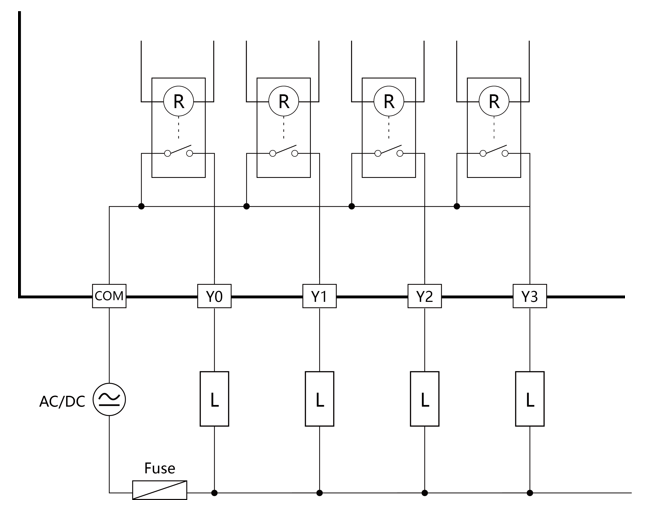
Single-End Relay Output Circuit
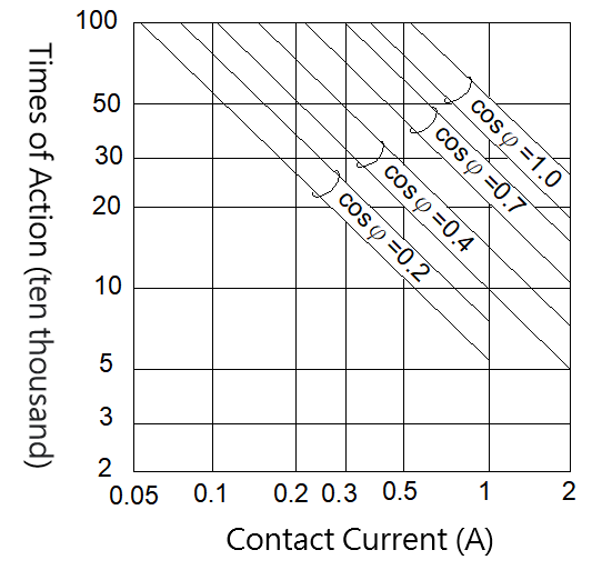
Relay life at different currents and phases
6-2-2 Structure and Wiring of Single-End Transistor SINK/SOURCE Output Circuit
The transistor contacts are divided into SINK and SOURCE output circuits. Each transistor contact can provide a max current of 0.1A. The max current limit of the output common point of the transistor can be divided into 1.6A current.
- Transistor Single-End SINK Output
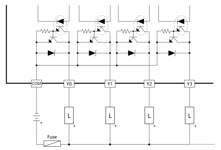
Transistor Single-End SINK Output
- Transistor Single-End SOURCE Output
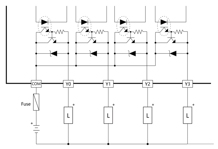
Transistor Single-End SOURCE Output
6-3 Speed up the Single-End Transistor Output Circuit
Either with the SINK or SOURCE structure in single-end output transistor circuit, when the transistor switches from ON to OFF, the junction capacitor between transistor CE electrodes should be charged to near the load voltage VDD before it can stop the current running through the photocoupler inside the load, which increase the OFF time and decrease the response speed. This problem can be solved by adding a Dummy load to accelerate charging rate and speed up the working frequency of transistor output. For the transistor output in M-PLC, Dummy load that are added to the high- and medium-speed transistor output and generate a load current of 20~50mA is adequate. For low-speed transistor where its driving capability (0.1A) but speed is concerned, adding a Dummy load only decreases its driving capability without any significant improvement and hence is not recommended. The following diagram shows how to add a Dummy load to SINK and SOURCE transistor output. (only applicable to high and medium-speed)
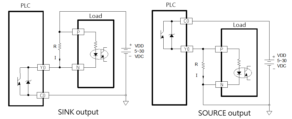
Speed up the Single-End Transistor Output Circuit
6-4 Output Device Protection and Noise Suppression in DO Circuit
Since the digital output circuits are mainly used for the ON/OFF switching operation, the output components such as relays, transistors and TRIAC can be deemed as kinds of switch components. Normally, surge currents or counter-electromotive force voltages are generated during the ON/OFF operation of these switch components. The effect of surge currents or counter-electromotive force voltages is particularly serious when heavy capacitive or inductive loads are incorporated, which may cause damage to the output components or generate noises in other electronic circuits and equipment. Among those three M-PLC output components, where TRIAC require no special treatment because of their features of smaller rated current, zero cross in ON/OFF, and built-in protection circuits, special consideration should be given to relays and transistors when they are used in high power applications or connected with capacitive or inductive loads and are described in the following:
6-4-1 Protection of Relay Contacts and Noise Suppression
Because the relay contacts are used to contact switch components having extremely low resistance, the surge current IR generated instantly upon turning on the relay is normally pretty strong (even if the steady load current is very small). Under such strong surge, the contact tends to melt and stick due to extreme temperature in such a way that the relay cannot trip when it is disconnected. In addition, when the relay connections are OFF, large di/dt is generated because of the instantaneous change from low resistance to open circuit (∞) soon after following the tripping of contact. As a result, an extremely strong counter-electromotive force voltage is induced, which creates sparks between the electrodes of two relay contacts and results in poor contact due to carbon deposits. Among those three output components, either in ON or OFF state, very serious interference can be caused by the surge current or the counter-electromotive of the relay. The solutions to this problem are listed as follows:
Suppression of Surge Current
Connect a small resistor R in series to lower the surge current, but note that too large R will affect the driving capability or cause too much voltage drop.
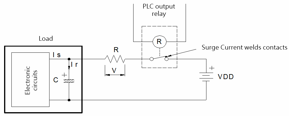
Ir max of relay in M Series PLC = 2A
Suppression of Counter-Electromotive Force
For the inductive load, whether in AC or DC power, suppression devices must be connected in parallel to both its ends to protect the relay contacts and lower noise interference. The schematic diagrams for AC and DC powers are shown below, respectively:
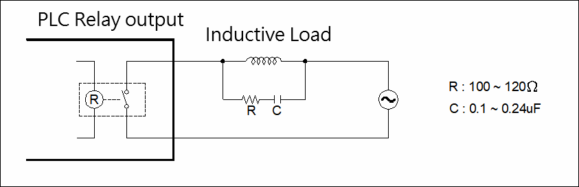
Scheme of AC power load
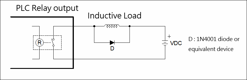
Suppress by a diode in DC power load (for low power)
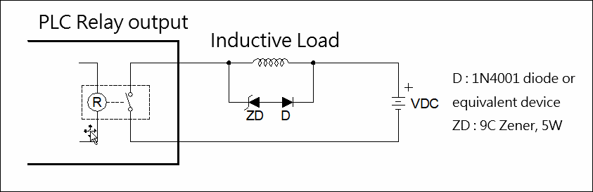
Suppress by a diode + Zener in DC power load (for high power and frequent ON/OFF)
6-4-2 Protection of Transistor Output and Noise Suppression
The transistor output in M Series PLC already includes Zener diode for counter-electromotive force, which is sufficient for low power inductive load and medium frequency of ON/OFF application. In conditions of high power or frequent ON/OFF, please construct another suppression circuit to lower noise interference and prevent voltage from exceeding the limit or overheating that may damage the transistor output circuit.
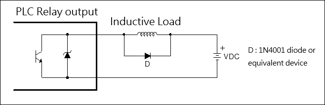
Suppress by a diode (for low power)
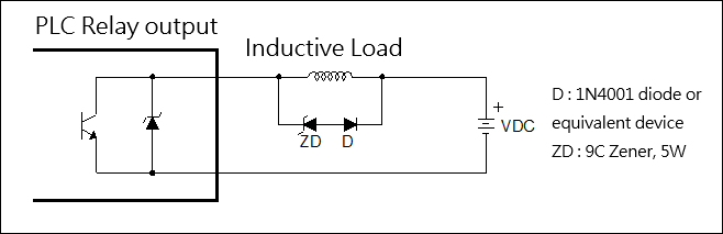
Suppress by a diode + Zener (high power and frequent ON/OFF)
Tip: press ← → to switch chapters, Ctrl+K to search