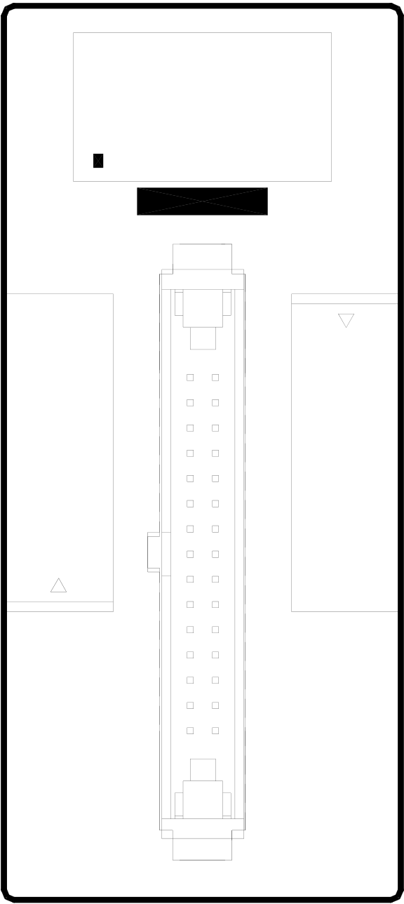
FBs-32DGI is a multiplex input module. One 32DGI module can support up to 32 digits thumbwheel switch or 128
discrete switch inputs. Thanks to the I/O control chip that incorporated in this module, the update rate of the input status is
irrelevant to CPU scan time. The input refresh time of this module is mere 10 mS. Owing to the scan nature of PLC,
though the multiplex input task is not performed by CPU, the over-all refresh time of this input module is still constrained
by the CPU scan time if the scan time is larger than 10 mS.
|
Appearance |
POW
FBs-32DGI
FG 24V+
24V- NC
D0 D1
D2 D3
D4 D5
D6 D7
D8 D9
D10 D11
D12 D13
D14 D15
NC S1
S2 S3
S4 S5
S6 S7
S8 NC
By using the multiplex input, users only need to connect the FBs-32DGI with 24 wires to achieve 32-digit inputs (or
128 switch points). While FBs-32DGI is only 4cm wide, it is a truly high-density, low-cost and labor-saving solution.
17.1 FBs-32DGI Specifications
|
Item |
Specification |
Remarks |
|
Input points |
32-digit DIP/128 independent switch points |
|
|
Occupied Resources |
8 IRs |
|
|
Connector |
30-pin boxed header |
|
|
Control signal |
Column Output– 8 dots SINK (NPN) output Row Output– 16 dots SOURCE output |
|
|
Refresh rate |
10mS |
|
|
Insulation |
Transformer (power) and optical separation (contact signal) |
|
|
Status indicator |
5VPWR LED indicator |
|
|
Power supply and consumption |
24V-15%/+20%, 40mA |
|
|
Internal current |
5V, 14mA |
|
|
Working temperature |
0 – 60°C |
|
|
Storage temperature |
20 – 80°C |
|
|
Dimensions |
40(W)×90(H)×80(D) mm |
|
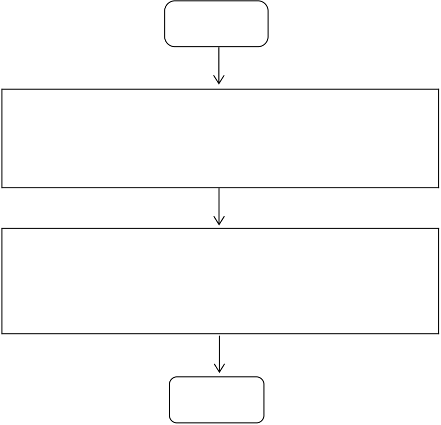
17.2 The Procedure of Using FBs-32DGI Module |
Start
Connect input signals to the DIP/switch point
according to the FBs-32DGI pin layout and connect
a 24VDC source to the module.
Read values from the analog/digital IR
R3840~R3903 to retrieve the digital input reading of
the DIP/switch point.
End
|
17.3 FBs-32DGI I/O Address |
Each FBs-32DGI module occupies 8 IRs (R3840~R3903) for I/O address. In general, WinProladder will automatically detect and calculate the actual I/O address occupied by the module installed on the system after connecting to the PLC. Users may refer to the I/O Module Number Configuration provided by WinProladder in order to find out the exact I/O address of each expansion module to facilitate programming.
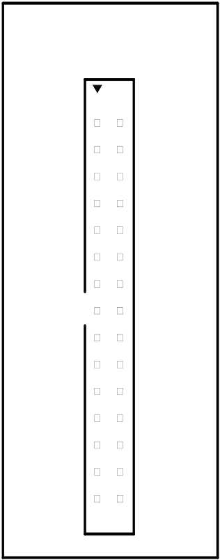
17.4FBs-32DGI Hardware Description
|
FBs-32DGI pin layout |
|
FBS-32DGI |
|
|||||||||||||||||||||||||||||||||||||||||||||||||||||||||||||||||||
|
FG |
I |
2 |
24V+ |
|||||||||||||||||||||||||||||||||||||||||||||||||||||||||||||||||
|
24V- |
NC |
|||||||||||||||||||||||||||||||||||||||||||||||||||||||||||||||||||
|
D4 |
D5 |
|||||||||||||||||||||||||||||||||||||||||||||||||||||||||||||||||||
|
D6 |
D7 |
|||||||||||||||||||||||||||||||||||||||||||||||||||||||||||||||||||
|
D8 |
D9 |
|||||||||||||||||||||||||||||||||||||||||||||||||||||||||||||||||||
|
D10 |
D11 |
|||||||||||||||||||||||||||||||||||||||||||||||||||||||||||||||||||
|
D12 |
D13 |
|||||||||||||||||||||||||||||||||||||||||||||||||||||||||||||||||||
|
D14 |
D15 |
|||||||||||||||||||||||||||||||||||||||||||||||||||||||||||||||||||
|
NC |
S1 |
|||||||||||||||||||||||||||||||||||||||||||||||||||||||||||||||||||
|
S4 |
S5 |
|||||||||||||||||||||||||||||||||||||||||||||||||||||||||||||||||||
|
S6 |
S7 |
|||||||||||||||||||||||||||||||||||||||||||||||||||||||||||||||||||
|
S8 |
29 |
30 |
NC |
|||||||||||||||||||||||||||||||||||||||||||||||||||||||||||||||||
|
[Aerial View] |
||||||||||||||||||||||||||||||||||||||||||||||||||||||||||||||||||||
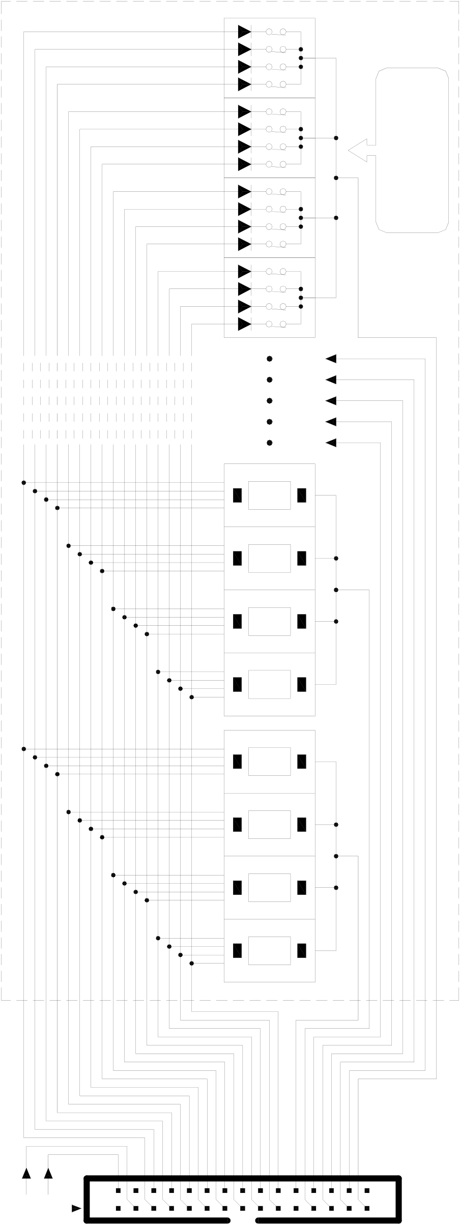
The I/O control chip built in the module multiplexes the 32 digits of thumbwheel switch or 128 discrete switch inputs by eight times scan, each scan reads in 4 digits of thumbwheel switch or 16 discrete switch inputs. The input selection signals S1~S8 listed in the above table are all low active output signal(NPN output). The multiplex data input signals D0~D15 are sink type input signals. Each times of scan, data are read from D0~D15 inputs and stored in I/O control chip.
The status of 32 digits of thumbwheel switch or 128 discrete switch inputs are directly mapped to 8 input registers as shown in following table. The IR is the first input register allocated for corresponding module (IR’s range is R3840~R3903).
|
DIP switch input |
|
IR |
D15-D12 |
D11-D8 |
D7-D4 |
D3-D0 |
|
IR+0 |
DIG3 |
DIG2 |
DIG1 |
DIG0 |
|
IR+1 |
DIG7 |
DIG6 |
DIG5 |
DIG4 |
|
IR+2 |
DIG11 |
DIG10 |
DIG9 |
DIG8 |
|
IR+3 |
DIG15 |
DIG14 |
DIG13 |
DIG12 |
|
IR+4 |
DIG19 |
DIG18 |
DIG17 |
DIG16 |
|
IR+5 |
DIG23 |
DIG22 |
DIG21 |
DIG20 |
|
IR+6 |
DIG27 |
DIG26 |
DIG25 |
DIG24 |
|
IR+7 |
DIG31 |
DIG30 |
DIG29 |
DIG28 |
Single point switch input
|
IR |
D15 |
D14 |
D13 |
D12 |
D11 |
D10 |
D9 |
D8 |
D7 |
D6 |
D5 |
D4 |
D3 |
D2 |
D1 |
D0 |
|
IR+0 |
I15 |
I14 |
I13 |
I12 |
I11 |
I10 |
I9 |
I8 |
I7 |
I6 |
I5 |
I4 |
I3 |
I2 |
I1 |
I0 |
|
IR+1 |
I31 – I16 |
|||||||||||||||
|
IR+2 |
I47 – I32 |
|||||||||||||||
|
IR+3 |
I63 – I48 |
|||||||||||||||
|
IR+4 |
I79- I64 |
|||||||||||||||
|
IR+5 |
I95 – I80 |
|||||||||||||||
|
IR+6 |
I111- I96 |
|||||||||||||||
|
IR+7 |
I127 – I112 |
|||||||||||||||
|
17.5 FBs-32DGI Input Circuit Diagram |
|
Thumbwheel switch module |
24V+ |
NC |
D1 |
D3 |
D5 |
D0 |
D11 |
8 |
S3 |
S5 |
S8 |
NC |
Connection for |
independent |
switch input |
|||
|
D4 |
||||||||||||||||||
|
D8 |
S6S7 |
|||||||||||||||||
|
D12 |
||||||||||||||||||
|
D0 |
S5 |
|||||||||||||||||
|
S3S4 |
||||||||||||||||||
|
D4 |
8 |
S2 |
||||||||||||||||
|
D8 |
8 |
S1 |
||||||||||||||||
|
D12 |
||||||||||||||||||
|
8 |
||||||||||||||||||
|
D0 |
||||||||||||||||||
|
8 |
||||||||||||||||||
|
D4 |
||||||||||||||||||
|
8 |
||||||||||||||||||
|
D8 |
8 |
S7 |
||||||||||||||||
|
D12 |
||||||||||||||||||
|
8 |
||||||||||||||||||
|
D7 |
D9 |
|||||||||||||||||
|
D13 |
D15 |
S1 |
||||||||||||||||
|
24V- |
24V+ |
2 |
FG |
24V- |
D0 |
D2 |
D4 |
D6 |
D8 |
D10 |
D12 |
D14 |
NC |
S2 |
S4 |
S6 |
S8 |
30 |
|
1 |
||||||||||||||||||
|
29 |
Tip: press ← → to switch chapters, Ctrl+K to search